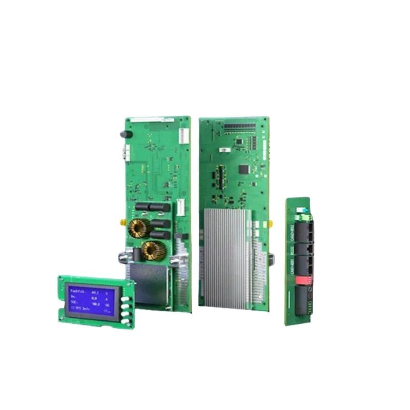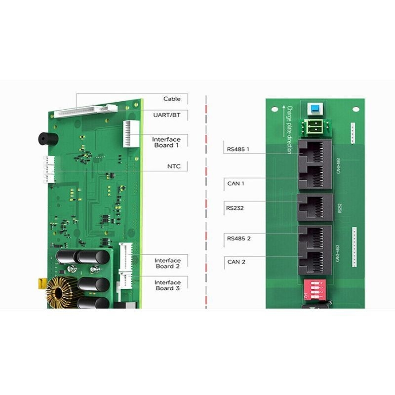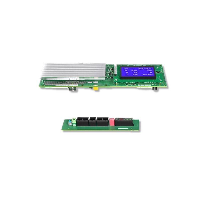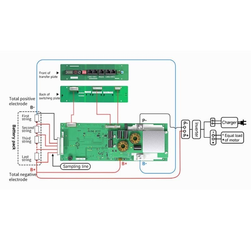
OEM Automotive PCBA Board PCBA PCB Assembly Smart Lifepo4 Battery PCBA
-
Highlight
OEM Automotive PCBA
,Automotive PCBA Board
,PCBA PCB Assembly Smart
-
Base MaterialFR4
-
Copper Thickness1oz
-
Board ThicknessAs Your Required
-
Min. Hole SizeStandard Or Custom
-
Min. Line WidthStandard Or Custom
-
Min. Line SpacingStandard Or Custom
-
Surface FinishingStandard Or Custom
-
Board SizeStandard Or Custom
-
Product NamePCBA Board
-
KeywordsPCBA OEM PCB Assembly
-
CertificateROSH. ISO9001
-
ApplicationBMS
-
ServiceOne-Stop OEM Service
-
Testing Service100% E-testing
-
MOQ1 PCS
-
ColorRed Blue Green Black White
-
PackageStandard Package
-
Our ServiceTurnkey PCBA
-
Place of OriginChongqing, China
-
Brand NameXZH
-
Model NumberXZH PCBs
-
Minimum Order Quantity10 pieces
-
Price$25.00/pieces 10-9999 pieces
OEM Automotive PCBA Board PCBA PCB Assembly Smart Lifepo4 Battery PCBA
PCBs Manufacturer Smart bms 4s 8s 16s 48v Industrial Grade Inverter Lifepo4 Battery PCBA Board
XZH: Your One-Stop ODM/OEM Solution Provider
Capabiity
|
Description
|
Technology & Capabilities
|
|
|
|
|
||||
|
1. Product Range
|
Rigid PCBs from 2- 24 layers, HDI; Aluminium base
|
|
|
|
|
||||
|
2. Min. Board Thickness
|
2 layer
|
4 layer
|
6 layer
|
8 layer
|
10 layer
|
||||
|
|
min. 0.2 mm
|
0.4 mm
|
1 mm
|
1.2 mm
|
1.5 mm
|
||||
|
|
12 & 14 layer
|
16 layer
|
18 layer
|
20 layer
|
22 & 24 layer
|
||||
|
|
1.6 mm
|
1.7 mm
|
1.8 mm
|
2.2 mm
|
2.6 mm
|
||||
|
3. Max. Board Size
|
610 x 1200 mm
|
|
|
|
|
||||
|
4. Base Material
|
FR-4 Glass Epoxy laminate, Aluminium base, RCC
|
|
|
|
|
||||
|
5. Surface Finish Treatment
|
Electroless nickel Immersion gold ( Electoless Ni/Au). Organic Solerability Preservatives ( OSP or Entek). Hot Air Leveling ( Lead- Free, RoHS). Carbon Ink. Peelable Mask. Gold Fingers. Immersion Silve. Immersion Tin. Flash gold ( Electrolytic)
|
|
|
|
|
||||
|
6. Major Laminate
|
King Boad (KB-6150). ShengYi (S1141; S1170). Arion. YGA-1-1; Rogers and others.
|
|
|
|
|
||||
|
7. Via Holes
|
Copper PTH/ Blind Via/ Buried Via/ HDI 2+N+2 with IVH
|
|
|
|
|
||||
|
8. Copper Foil Thickness
|
18um/ 35um/ 70um~245um (outer layer 0.5oz~7oz)
18um/ 35um/ 70um~ 210um (inner layer 0.5oz~6oz)
|
|
|
|
|
||||
|
9. Min. Via Size and Type
|
Dia. 0.15mm (Finished).
Aspect Ratiao = 12; HDI holes (<0.10mm)
|
|
|
|
|
||||
|
10. Min. Line Width & Spacing
|
0.75 mm/ 0.10mm ( 3mil/ 4mil)
|
|
|
|
|
||||
|
11. Min Via Hole Size & Pad
|
Via: Dia, 0.2mm/ pad. dia. 0.4mm; HDI<0.10mm via
|
|
|
|
|
||||
|
12. Impedance I Control Tol.
|
+/- 10% ( min. +/- 7 Ohm)
|
|
|
|
|
||||
|
13. Solder Mask
|
Liquid Photo- Image (LPI)
|
|
|
|
|
||||
|
14. Profiling
|
CNC Routing, V- Cutting, Punching, Push back punching, Connector chamfering
|
|
|
|
|
||||
|
15. Capacity
|
100 k㎡ output monthly
|
|
|
|
|
||||
|
Item
|
Capability
|
|
Base material
|
FR4,High-TG FR4,CEM3,aluminum, High Frequencey frequency(Rogers,Taconic,Aron,PTFE,F4B)
|
|
Layers
|
1-4 Layers(Alunimum), 1-32 layers(FR4)
|
|
Copper Thickness
|
0.5oz, 1oz, 2oz, 3oz,4oz
|
|
Dielectric Thickness
|
0.05mm, 0.075mm, 0.1mm,0.15mm,0.2mm
|
|
board Core Thickness
|
0.4mm,0.6mm, 0.8mm, 1.0mm, 1.2mm,
1.5mm, 2.0mm, 3.0mm and 3.2mm |
|
Board Thickness
|
0.4mm - 4.0mm
|
|
Thickness Tolerance
|
+/-10%
|
|
Aluminum Machining
|
Drilling, Tapping, Milling, Routing, Die-Punching,
Break-off tab available |
|
Min Hole
|
0.2 mm
|
|
Min Track Width
|
0.2mm (8mil)
|
|
Min Track Gap
|
0.2mm (8mil)
|
|
Min SMD Pad Pitch
|
0.2mm (8mil)
|
|
Surface Finishing
|
HASL lead free,ENIG,Plated Gold,Immersion Gold,OSP
|
|
Solder Mask Color
|
Green, Blue, Black, White, Yellow, Red, Matt Green, Matt Black, Matt Blue
|
|
Legend Color
|
Black, White etc
|
|
Assembly Types
|
Surface mount
Thro-hole Mixed technology (SMT & Thru-hole) Single or double sided placement Conformal coating Shield cover assembly for EMI emission control |
|
Parts Procurement
|
Full Turnkey
Partial Turnkey Kitted/Consigned |
|
Component types
|
SMT 01005 or larger
BGA 0.4mm pitch, POP (Package on Package) WLCSP 0.35mm pitch Hard metric connectors Cable & wire |
|
SMT Parts Presentation
|
Bulk
Cut tape Partial reel Reel Tube Tray |
|
Stencils
|
Laser-cut stainless steel
|
|
Other Techniques
|
Free DFM Review
Box Build Assembly 100% AOI test and X-ray test for BGA IC programming Components cost-down Function test as custom Protection technology |
Customer Services
PCB Service
XZH Supply single-side, double –side board, multilayer boards (1-20 layers), Boards type:Rigid PCB(CEM, FR4), Flexible PCB, Rigid-Flex PCB, MCPCB(Aluminum PCB), Ceramic PCB, RF PCB, etc.
PCB Assembly&Components Sourcing
XZH offer Printed Circuit Board Assembly ,components Sourcing and complete solutions. what we can always gurantee is the best quality,competitive price and best service.
More Details or Other requirements welcome to Email and Chat with us.
Company Profile
Founded in 2014, XZH Technology Co., Ltd is a reputable entity, known for its strong technical team, comprehensive quality assurance systems, and cutting-edge analytical instruments. As a specialized PCB manufacturer, our products serve a wide range of applications across consumer electronics, telecommunications, medical equipment, and industrial sectors, enjoying robust demand in European and Southeast Asian markets.
Our holistic service offerings encompass schematic design, board layout, component sourcing, firmware design, mechanical design, PCBA, and chip cloning. Additionally, we extend our services to component procurement, PCB and FPC assembly, packaging, and logistics, ensuring a seamless one-stop solution for our clients. We pride ourselves on sourcing high-quality raw materials and key components from renowned suppliers such as Sharp, Toshiba, ST, Samsung, Infineon, JRC, and NEC, further underscoring our commitment to excellence.
Our facilities, certified by ISO 9001:2000 and ISO 14001:2004, span 2,000 square meters and are staffed by 300 skilled workers. We boast a production capacity of 10,000 square meters of PCB and 5,000 square meters of PCB FPC monthly. Our commitment to quality is reflected in our rigorous QC processes, supported by 30 experienced auditors and advanced testing equipment like AOI, BGA X-ray, and PCB E-test, ensuring compliance with IECO-HSPM QC 080000, CE, UL, and RoHS standards.
Aiming for "Professional Management, Large-scale Industry, International Market" as our strategic goal, we invite you to explore partnership opportunities with us for detailed insights into our services and capabilities.
Certifications
Exhibition
Our Advantages
Product Leading Time
|
|
Sample Lead time
|
Mass production lead time
|
||
|
Single sided PCB
|
1~3 days
|
4~7 days
|
||
|
Double sided PCB
|
2~5 days
|
7~10 days
|
||
|
Multilayer PCB
|
7~8 days
|
10~15 days
|
||
|
PCB Assembly
|
8~15 days
|
2~4 weeks
|
||
|
Delivery time
|
3-7 days
|
3-7 days
|
||
|
Package: Anti-static Package with carton
|
|
|
||
FAQ
Q1:Are my design files secure when I send them to you?
A:Your files held in complete safety and security. Your files are never
shared nor will any third parties have access to your design files. Fulltronics can sign a Non-disclosure agreement before sending files.
shared nor will any third parties have access to your design files. Fulltronics can sign a Non-disclosure agreement before sending files.
Q2:For small quantity orders, can you produce prototype PCBs?
A:Yes, XZH PCB can produce prototypes. but the greater the quantity, the greater the cost savings.
Q3:Do you have after-sales product servicing available for your customers?
A:Yes, for any quality problems XZH PCB will take our responsibility to solve them for you at any time. What we can always guarantee is our best service, high quality with competitive price.
Q4:What's files do you need in the PCBA projects?
A:Exclude the pcb file, the PNP(Pick and Place) file and Components Position file also needed.
Q5: Does our product will be tested before shipment?
A: Yes, we could provide Function Circuit Testing if you provide us the testing methods.
